


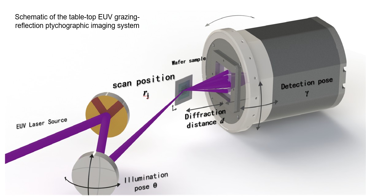
Full-pose self-calibrated EUV grazing-reflection ptychography system.
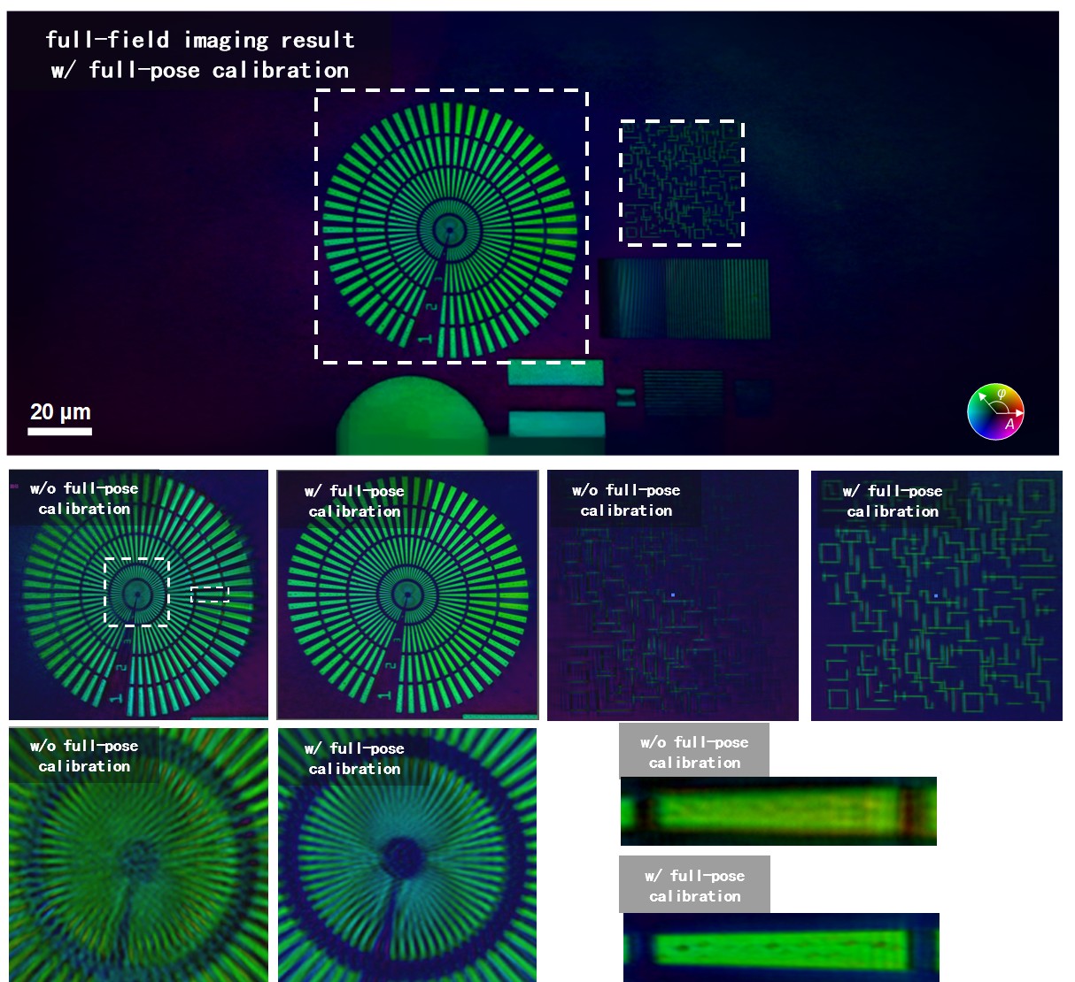
Imaging results of a customized wafer sample.
GA, UNITED STATES, September 22, 2026 /EINPresswire.com/ -- Researchers have developed a table-top extreme-ultraviolet grazing-reflection ptychography system with full-pose self-calibration for high-precision semiconductor metrology. By combining holistic system modeling, feature-domain loss evaluation, and automatic-differentiation-based phase retrieval, the method jointly calibrates critical system parameters. Experiments successfully resolve 43.5-nm half-pitch structures in real chip samples while correcting geometric distortions and identifying defects, offering a practical route toward nondestructive nanoscale semiconductor inspection.
The diffraction limit has long imposed a fundamental constraint on optical imaging, making shorter-wavelength illumination a natural route toward higher spatial resolution. As semiconductor feature sizes continue to shrink and extreme-ultraviolet (EUV) lithography advances toward increasingly sophisticated manufacturing nodes, the demand for high-resolution EUV inspection and metrology is becoming particularly urgent.
However, imaging at EUV wavelengths presents substantial technical challenges. Strong material absorption makes conventional transmissive optics impractical, while reflective EUV optics require sophisticated multilayer coatings and extremely stringent surface quality. Ptychography provides an attractive lensless alternative. By scanning overlapping illumination regions across a sample and computationally recovering the complex wavefield from the resulting diffraction patterns, ptychography can achieve a numerical aperture determined primarily by the diffraction geometry and detector size, allowing the imaging resolution to approach the diffraction limit.
Reflection-mode EUV ptychography is particularly promising for semiconductor inspection, but its practical implementation has long been limited by system alignment and calibration. In a grazing-reflection geometry with a reflection angle of approximately 70 degrees, the detector is positioned normal to the outgoing beam while remaining strongly tilted with respect to the sample surface. As a result, diffraction signals are nonuniformly sampled on the Ewald sphere, producing pronounced distortions that depend sensitively on the system geometry. Conventional calibration approaches generally correct only one or two pose parameters while neglecting other coupled errors, leaving residual artifacts that compromise quantitative imaging and high-precision metrology.
In a new paper published in Light: Advanced Manufacturing, a research team led by Professor Yishi Shi at the University of Chinese Academy of Sciences developed a table-top 17.9-nm EUV grazing-reflection ptychography system capable of full-pose self-calibration. The work establishes a comprehensive imaging framework that combines full-system forward modeling, feature-domain loss evaluation, and automatic-differentiation-based optimization.
At the core of the method is a unified physical model describing the mapping between the Ewald sphere and the tilted detector plane. Critical experimental parameters—including the diffraction distance, three-dimensional illumination angle, three-dimensional detector pose, and scanning positions—are incorporated into the ptychographic forward model rather than calibrated independently. The researchers then use a feature-domain loss to assess data fidelity and automatic differentiation to jointly recover the sample, illumination probe, and system pose parameters.
This holistic calibration strategy substantially improves reconstruction fidelity. Experiments on a customized wafer sample show that full-pose self-calibration provides the highest image quality among the investigated reconstruction approaches. Fine structures near the center of a Siemens star and point-like defects can be clearly resolved, while geometric distortions of the wafer patterns are significantly suppressed, enabling more accurate critical-dimension measurements.
The researchers further demonstrated the system on a real chip sample. The reconstructed image clearly resolves grating structures with a 43.5-nm half-pitch, in agreement with scanning electron microscopy measurements. The EUV ptychographic system also successfully identifies contamination and scratch defects on the chip, demonstrating its capability for practical, nondestructive inspection of semiconductor structures.
Beyond the experimental demonstrations, the study systematically investigates several factors governing the performance and robustness of reflection ptychography. These analyses include the advantages of feature-domain loss functions for EUV phase retrieval, the sensitivity of image reconstruction to system-parameter errors under different experimental geometries, coupling effects among pose parameters during full-pose self-calibration, and reconstruction performance under low-dose conditions. These investigations provide useful guidance for both algorithm development and system design in practical ptychographic imaging.
By integrating physical modeling, computational optimization, and experimental validation, the work provides a systematic solution to one of the central challenges in reflection ptychography. The proposed full-pose self-calibration strategy eliminates the need for highly precise hardware alignment while maintaining high reconstruction fidelity and computational efficiency. Beyond EUV imaging, the underlying methodology could also provide a general framework for reflective or tilted-geometry ptychography using visible light, X-rays, and electron beams.
The combination of a compact table-top EUV source, comprehensive self-calibration, and nanometer-scale imaging capability points toward practical applications in high-resolution micro- and nanoscale inspection. In particular, the approach may enable nondestructive structural characterization of advanced semiconductor devices, including emerging three-dimensional heterogeneous integrated structures, and help accelerate the translation of EUV ptychography from laboratory demonstrations toward industrial semiconductor metrology.
References
DOI
10.37188/lam.2026.112
Original Source URL
https://doi.org/10.37188/lam.2026.112
Funding information
This work was supported by the National Key Research and Development Program of China (Grant No.2021YFB3602604), National Natural Science Foundation of China (62131011), and Fundamental Research Funds for Central Universities (E3ET6201X2).
About Light: Advanced Manufacturing
The Light: Advanced Manufacturing is a new, highly selective, open-access, and free of charge international sister journal of the Nature Journal Light: Science & Applications. It will primarily publish innovative research in all modern areas of preferred light-based manufacturing, including fundamental and applied research as well as industrial innovations.
Lucy Wang
BioDesign Research
email us here
Legal Disclaimer:
EIN Presswire provides this news content "as is" without warranty of any kind. We do not accept any responsibility or liability for the accuracy, content, images, videos, licenses, completeness, legality, or reliability of the information contained in this article. If you have any complaints or copyright issues related to this article, kindly contact the author above.
